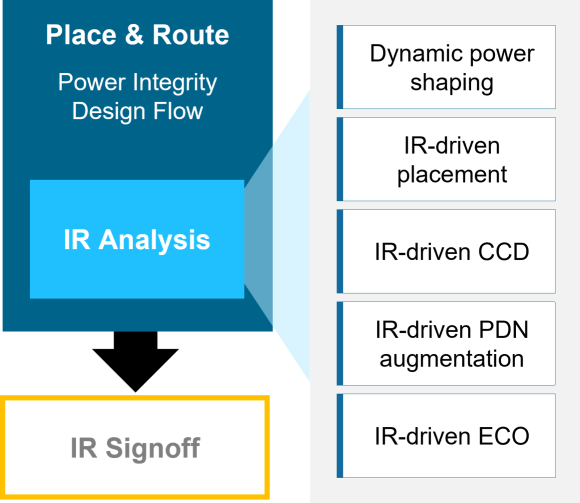
ASIC PDN (Power Distribution Network) signoff involves verifying that the power delivery network on an ASIC design meets all requirements for power integrity, electromigration, and other critical factors. This process ensures the power supply reaches the chip’s internal components reliably and without excessive voltage drops, noise, or other issues that could compromise performance or reliability. There are several aspects to this analysis.
Key Aspects of ASIC PDN Signoff:
IR Drop Analysis:
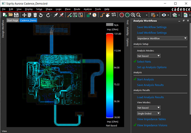
This analysis checks for voltage drops across the PDN, ensuring that the voltage at the Point of Load (POL) meets the requirements of the load. IR drop looks at the potential for the voltage on a transistor not being adequate and impacting timing and potential functional integrity. Electromigration Analysis: This analysis predicts the likelihood of metal traces on the chip failing due to electromigration, a phenomenon where atoms of the metal move under the influence of electric currents. Electromigration looks at the likelihood that traces will age over time resulting in devices that prematurely fail.
Noise Analysis: This analysis evaluates the noise on the power rails and their impact on sensitive circuitry. Noise analysis looks to see if sensitive circuitry will be affected either directly or through coupling.
Thermal Analysis: This analysis assesses the temperature distribution on the chip and the PDN, ensuring that the chip doesn’t overheat.
Power Supply Ripple and Noise Analysis: This analysis verifies that the voltage at the POL is within the acceptable range, considering factors like simultaneous switching noise and other disturbances.
Signoff Tools and Methods:
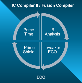
EDA tools: Various Electronic Design Automation (EDA) tools are used to perform these analyses, such as Cadence Voltus IC Power Integrity Solution.
Simulation: Simulation models are used to predict the behavior of the PDN under various operating conditions.
Power integrity analysis: This analysis helps ensure that the power seen at the components is equal to the intended output from the power regulator.
Getting power around a semiconductor device is complicated and expensive. It generally starts at a power supply and transferred by wires to a printed circuit board. Attached to that board are one or more ICs. Traces on the PCB connect from the pads where the power supply wires are connected to the pad where power will be transferred to the chip. Those PCB traces may also involve vias that go through the PCB. To go from the chip pad into the chip will involve some kind pin or bump and that has to be connected to the semiconductor surface – often involving a wire or other metal conductor and solder.
Then a series of metal layer traces and vias, and potentially traces within the silicon, connect the transistors to the supply. Along that path, a set of resistances, capacitance and inductances are inherited that mean that what appears at the transistor is not a perfect replication of what came out of the power supply.
Voltage regulators or converters may also be inserted anywhere along that path to provide the necessary voltages for various pieces of the circuit. In low power designs, switches may exist within the power supply to enable power to be removed from some parts of the circuit to reduce the leakage power. Because of peak current demands, capacitors may be added the retain enough charge to meet the instantaneous demand and are then recharged when less current is required.
Historically, the power delivery network (PDN) was overdesigned by adding significant margins to all aspects of the network, thus ensuring that timing or functional failures were not caused by an inadequate design. More recently, that level of margin can no longer be tolerated and so much more attention is being paid to the PDN and much more analysis is being performed on it. This is sometimes called power integrity analysis.