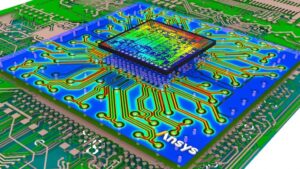
As Moore’s Law slows, the semiconductor industry is turning to advanced packaging to unlock new levels of performance, especially for AI, HPC, and 5G applications.
◯ IR-drop is the new bottleneck. With supply voltages dipping below 0.7 V, even a few millivolts of droop can wreck timing margins.
◯ Resistance is rising. As we scale to finer nodes, wires get thinner, longer, and far more resistive.
◯ Analysis is exploding. Modern PDN simulations deal with 60 – 100 billion electrical nodes. One misstep can collapse a design cycle.
◯ Early planning is everything. Fixing power integrity late in sign-off is too costly — floorplan-stage awareness is now critical.
💬 We’ve been solving for logic. We’ve been solving for leakage.
The next frontier? Solving for electrons themselves.
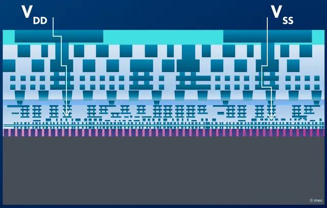
🔋 Backside Power Delivery (BSPDN) is the next big step.
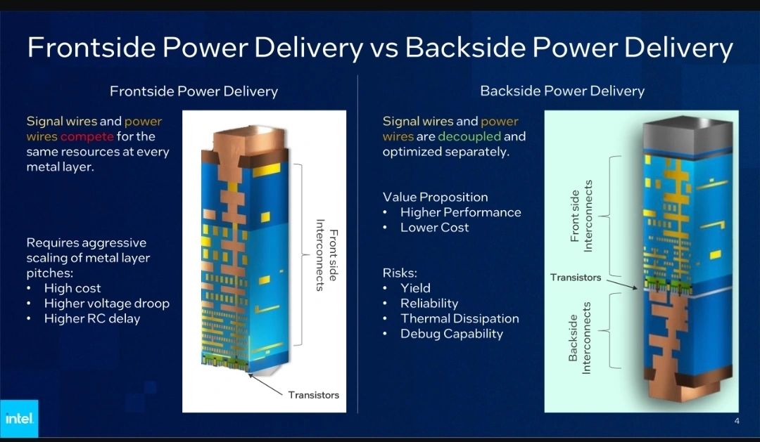
By routing power through the wafer’s back, BSPDN shortens the current path, cuts IR-drop, and frees up top-side metal for signals — a leap already being explored in Intel’s PowerVia and TSMC’s Angstrom-class (1.4 nm) nodes.
It’s coming up with great promise — but how much new innovation the ecosystem will need to make it mainstream is still an open question.
🔌 Backside Power Delivery (BPD)
A game-changer in CMOS scaling, BPD relocates power interconnects to the backside of the wafer, dramatically reducing voltage droop, improving power integrity, and freeing up the frontside for signal routing. Intel’s PowerVia and TSMC’s Super Power Rail are already pushing this into sub-2nm nodes. The result? Up to 30% reduction in power losses and fewer costly EUV lithography steps.
💡 The future of semiconductors isn’t just about shrinking transistors, it’s about smarter, more efficient packaging.
Traditional (Front-side):
┌─────────────────┐
│ Transistors │
│ Signal Metals │
│ Power Metals │ ← Power/signal compete for resources
│ │
└─────────────────┘
Backside Power:
┌─────────────────┐
│ Transistors │
│ Signal Metals │ ← Signals only (no power routing)
│ │
├─────────────────┤ ← Wafer thinning
│ Power Metals │ ← Dedicated power delivery
└─────────────────┘
Benefits of Backside Power (When Available):
- Reduced IR drop: Shorter paths to transistors
- Improved signal routing: More tracks available for signals
- Higher performance: Reduced power noise on critical paths
- Smaller area: Eliminates front-side power routing congestion
Who Has Backside Power Today?
- Intel: RibbonFET + PowerVia (20A/18A nodes)
- Samsung: Backside Power Delivery (SF2/SF2P)
- TSMC: Coming in N3E/N3P (not in initial N3B)
When to Expect Backside in TSMC:
- 2024-2025: N3E with initial backside features
- 2025-2026: N3P with optimized backside power
- N3B users: Stick with conventional power delivery

