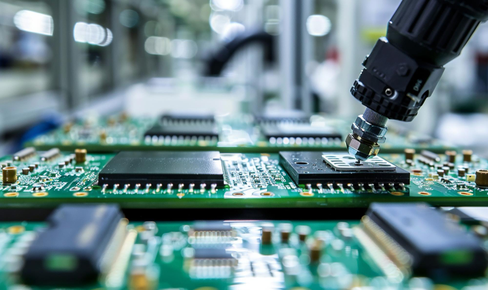
Turnkey solutions from RTL to GDS2.
Design Services Education and Training.
We provide expert power estimation services for cutting-edge ASIC nodes. Specializing in power analysis for designs at 5nm and below.
Offering turnkey solutions from RTL to GDS2 flows. Ensuring seamless ASIC design and smooth project execution.
Customized training to empower your team in ASIC design. Learn top techniques for power management and design optimization.
We are a team of seasoned professionals with years of experience in cutting-edge technology. Our expertise has been developed through work with both innovative startups and leading global brands. Here’s why we stand out:
We focus on low-power design strategies, incorporating multi-VDD techniques to reduce power consumption while maintaining performance.
We provide end-to-end services for the entire design flow, from RTL to GDSII, ensuring your designs are ready for manufacturing with accurate netlists and gate placements.
Our signal and power analysis services identify and resolve power inefficiencies and signal integrity issues, guaranteeing optimal design performance.
We offer ATPG services to generate test patterns that allow for efficient and thorough fault detection, improving the overall quality and reliability of your design.
We integrate full-chip designs, optimizing all blocks to work seamlessly together, ensuring high functionality and performance across the entire chip.
We specialize in block-level design, implementing individual blocks to meet specific requirements while ensuring overall chip-level efficiency and performance.
We specialize in creating tailored design flows that ensure a smooth and efficient process, from initial concept to final GDSII.
We integrate test structures like SCAN, BIST, and JTAG to verify the functionality and reliability of your design, ensuring robust and fault-free operation.
We manage engineering change orders (ECOs) to implement design modifications efficiently, including both metal-only and all-layer ECOs, ensuring fast and effective updates to your design.

Whether it is a stable 45nm or evergreen 28nm or cutting edge 2nm tech node, we can help you in achieve your targets.