Low Power Design Techniques in ASIC Physical Design
As the demand for energy-efficient integrated circuits continues to rise, low power design techniques have become a critical aspect of ASIC physical design. By employing strategies such as voltage scaling, clock gating, and power gating, designers can significantly reduce the power consumption of their chips without compromising performance. Additionally, optimizing the layout and interconnects can further minimize power dissipation, making it possible to create highly efficient ASICs that meet the stringent requirements of modern applications.

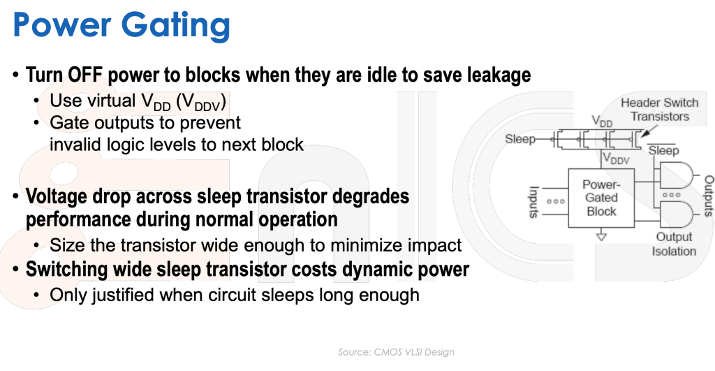
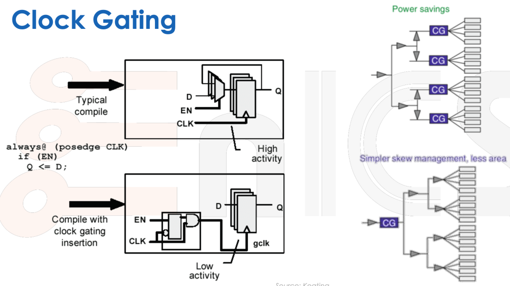
Clock Gating turns off power to an entire region, however, the leakage power is still being consumed.
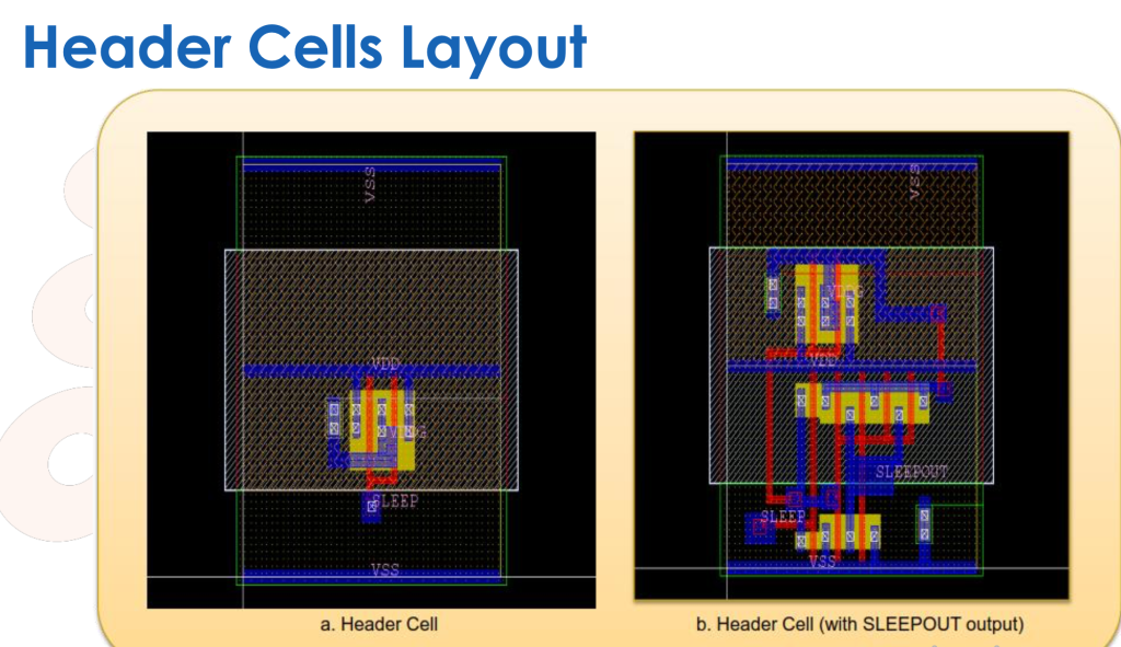
For Power Gating, the use of Power Switch Cells is necessary, as such, they can be Foot or Head Switches.