While closing IR drop within specified limits is a critical problem and challenge to solve for a smooth tapeout, the impact of IR drop is more than just timing closure or functional failure related. Understanding the science behind functional failures is the key to underline the significance of ensuring IR targets are met.
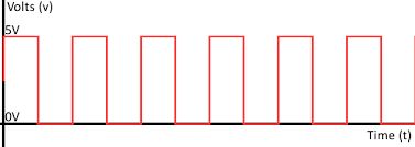
Imagine a clock waveform with an ideal 50% duty cycle at 1.0V source voltage from the power pads. Now, assuming that due to grid resistance, the driver sees a 10% voltage drop and only gets 0.9V on silicon. How does this impact the clock waveform?
Here’s a detailed breakdown of the impact of a 10% IR drop (from 1.0V to 0.9V) on a digital clock signal with 50% duty cycle, covering waveform integrity, timing, and power implications.
10% IR drop (to 0.9V) reduces the signal’s high level, increasing rise/fall times and propagation delays by ~10-20%. Noise margins degrade, raising susceptibility to errors. Dynamic power drops by 19%, but leakage may rise due to slower switching. Mitigations include decap insertion, power grid optimization, and voltage-domain isolation.”
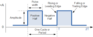
1. Voltage-Level Impact on Waveform
Original Signal:
- High (Logic ‘1’): 1.0V
- Low (Logic ‘0’): 0V (assumed)
- Duty Cycle: 50% (equal high/low durations).
After 10% IR Drop (0.9V):
- High (Logic ‘1’): Reduced to 0.9V (10% drop).
- Low (Logic ‘0’): Unaffected (remains 0V).
Waveform Changes:
- Amplitude Reduction: The high-level voltage is now 0.9V, shrinking the voltage swing (ΔV = 0.9V).
- Duty Cycle: Remains 50% (time spent high/low is unchanged, but noise margins degrade).
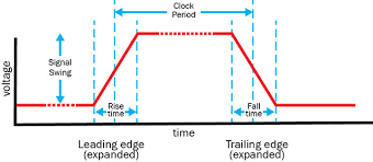
2. Timing and Signal Integrity Effects
A. Rise/Fall Times
Slower Transitions: Reduced voltage swing leads to:
- Longer rise/fall times due to weaker drive strength (current ∝ V).
- Example: A buffer’s slew rate degrades because ( I = \frac{C \cdot \Delta V}{\Delta t} ).
B. Propagation Delay
- Increased Delay:
Gate delays ((t_{pd})) scale with voltage:
[t_{pd} \propto \frac{V}{V – V_{th}} \quad \text{(Alpha-power law)}] - At 0.9V, delays increase by ~10-20% (depends on (V_{th})).
- Critical Paths: May violate setup/hold times, risking functional failures.
C. Noise Margins
- Reduced Noise Immunity:
- NMH (High noise margin) drops from (1.0V – V_{IH}) to (0.9V – V_{IH}).
- Higher susceptibility to crosstalk/ground bounce.
3. Power Implications
- Dynamic Power Reduction: [P_{\text{dynamic}} \propto C \cdot V^2 \cdot f]
- Power savings: ( (1.0^2 – 0.9^2) = 19\% ) lower dynamic power.
- Tradeoff: Performance loss (slower transitions).
- Leakage Power: May increase due to longer activity periods (slower switching).
4. Real-World Mitigation Techniques
A. Design Fixes
Decoupling Capacitors:
- Add decaps near noise-sensitive logic to stabilize voltage.
Power Grid Reinforcement:
- Widen power rails or use thicker metal layers.
Voltage Domains: - Isolate critical paths to higher-voltage domains.
B. Analysis Tools
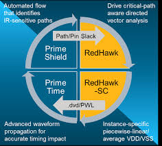
- IR Drop Analysis: Ansys RedHawk, Cadence Voltus.
- Timing Signoff: PrimeTime with voltage-aware derating.
Key Takeaways
- Waveform: Smaller swing, slower edges.
- Timing: Delays increase, risking setup/hold violations.
- Power: Dynamic power ↓, but leakage may ↑.
- Fix: Decaps, robust PDN, and voltage-aware STA.